


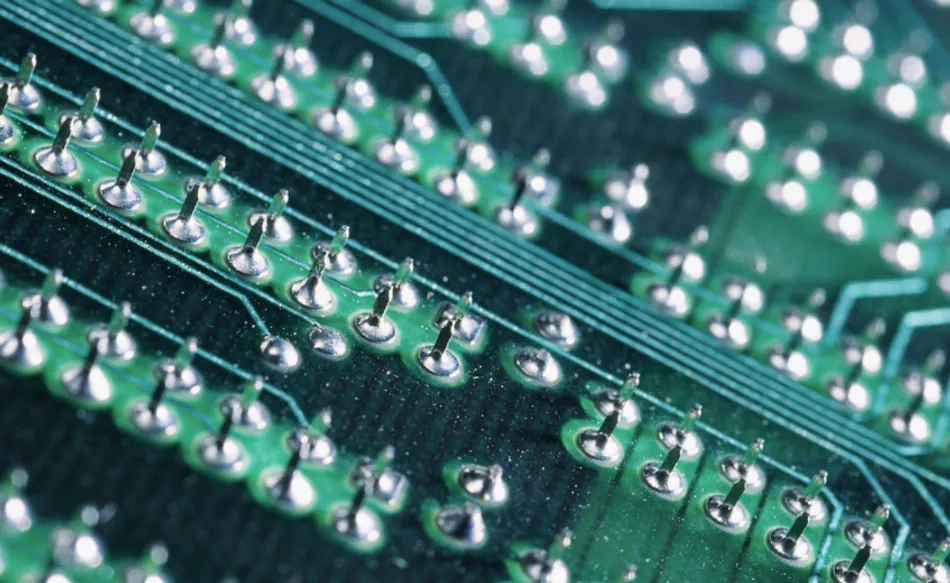
Solder reflow is a crucial process in the electronics industry, primarily utilized for attaching surface-mount components to printed circuit boards (PCBs). This process entails the application of solder paste to specific locations on a PCB, the placement of components on the paste, and subsequent heating of the assembly in a reflow oven. As the solder paste melts, it forms a dependable electrical and mechanical connection between the component and the PCB. The quality of these connections significantly impacts the performance and reliability of the final electronic product.
Throughout the solder reflow process, several factors influence the quality of the solder joint, including the composition of the solder paste, the type of reflow oven, and the temperature profile. Understanding these factors and their interactions is crucial for achieving optimal soldering results. This article delves deep into the solder reflow process, exploring its various aspects, challenges, and best practices. By providing a comprehensive understanding of the techniques and principles involved, it equips the reader with the knowledge to make informed decisions when working with solder reflow.
Reflow Soldering Process Step by Step
Preparing the PCB
To ensure high-quality solder joints, proper PCB cleaning is essential before solder reflow. The cleanliness of the PCB surface directly impacts the solder paste's ability to adhere to the board and form a reliable connection. Contamination, such as dust, grease, and oxidation, can result in soldering defects and reduced product reliability.
Several methods can be employed to clean PCBs before solder reflow, including ultrasonic cleaning, aqueous cleaning, and solvent cleaning. Ultrasonic cleaning utilizes high-frequency sound waves to eliminate contaminants, while aqueous cleaning relies on water-based solutions. Solvent cleaning involves the use of specialized chemicals to dissolve contaminants. Each method has its own set of advantages and disadvantages, influenced by factors such as the type and extent of contamination, PCB material, and environmental considerations
Following PCB cleaning, the subsequent step involves the application of solder paste. Solder paste is comprised of metal alloy particles, flux, and other additives that melt during reflow, establishing a bond between the PCB pads and component terminals. An essential aspect of solder paste application is the precise deposition of the paste onto the PCB pads, typically accomplished using a stencil printer.
Stencil Printing
Stencil printing plays a pivotal role in the solder reflow process by guaranteeing precise solder paste deposition onto the PCB pads. A meticulously crafted stencil is imperative for attaining superior solder joint quality. Stencils are commonly fabricated from stainless steel or polyimide film and feature apertures that correspond to the PCB pad layout. Once positioned on the PCB, solder paste is evenly distributed across the stencil using a squeegee, thereby filling the apertures and transferring the paste onto the pads.
Numerous factors impact the stencil printing process and the quality of solder paste deposition:
Stencil Design: The stencil's thickness and aperture dimensions must precisely match the PCB pad size and component requirements. Stencil thickness determines the amount of solder paste deposited on the pads, while aperture dimensions control the paste's lateral spread. A well-designed stencil reduces the risk of solder bridging and ensures sufficient solder on the pads.
The formula to calculate the approximate stencil thickness is as follows:
Area Ratio = Area of the pad / Area of the aperture walls = L * W / 2 * (L + W) * T/div>
Where, L = Length of Pad, W = Width of Pad, T = Thickness of Pad
Printing Parameters: The squeegee angle, pressure, and speed are crucial in stencil printing. Incorrect squeegee angles may result in incomplete aperture filling, while excessive pressure or speed can cause smearing or misalignment of the solder paste on the pads. Proper calibration and adjustment of these parameters ensure precise solder paste deposition.
Solder Paste Properties: The rheological properties of solder paste, such as viscosity and thixotropy, impact its flow through stencil apertures and adhesion to PCB pads. Solder paste must exhibit suitable viscosity and thixotropic behavior for consistent and accurate deposition. The paste's metal content, alloy composition, and particle size distribution also influence final solder joint quality.
Regular inspection and maintenance of the stencil printer are essential to prevent defects and maintain high-quality solder paste deposition. This involves cleaning the stencil to remove solder paste residue and verifying the alignment and accuracy of the printing process.
Pick and Place
The pick and place process is integral to the solder reflow procedure, involving the precise placement of surface mount components onto PCB pads coated with solder paste. This task is carried out by pick and place machines, also referred to as component placement systems. These machines utilize a blend of cameras, robotic arms, and vacuum nozzles to retrieve components from reels or trays and position them accurately onto the PCB.
Several factors contribute to the efficiency and accuracy of the pick and place process:
Component Recognition and Orientation: Modern pick and place machines utilize advanced vision systems to recognize components, determine their orientation, and ensure proper placement on the PCB. These systems can detect various component types, including passive components, integrated circuits, and connectors. Accurate component recognition is essential for avoiding placement errors such as tombstoning, skewing, and misalignment.
Placement Speed: The speed at which the machine picks up components and places them on the PCB significantly impacts production throughput. High-speed placement machines can handle tens of thousands of components per hour, while more flexible machines may have a lower placement rate but support a wider range of component types and sizes.
Machine Accuracy and Repeatability: The precision of the pick and place machine determines the accuracy of component placement on the PCB. High-precision machines can place components with micron-level accuracy, ensuring reliable solder joints and minimal defects during the reflow process. Repeatability refers to the machine's ability to consistently place components within a specified accuracy range, crucial for maintaining high-quality solder joints across multiple PCB assemblies.
Feeder Capacity and Changeover Time: The number of component feeders a machine can accommodate directly impacts its versatility and productivity. Machines with more feeder slots can handle a wide variety of components, reducing the need for frequent changeovers. Additionally, machines with quick changeover times minimize production downtime, enhancing overall efficiency.
Proper calibration and maintenance of the pick and place machine are essential for ensuring accurate component placement and minimizing defects during the solder reflow process. Regular calibration and maintenance procedures help maintain optimal machine performance and prevent production disruptions.
Solder Reflow Oven
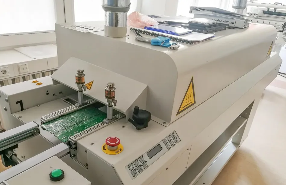
Solder reflow ovens are essential equipment utilized to heat solder paste and establish a robust connection between surface-mount components and the PCB. These ovens employ controlled temperature profiles to achieve optimal solder joint quality and reliability. The reflow process encompasses four primary phases: preheating, soaking, reflow, and cooling. Each phase is pivotal in achieving high-quality solder joints and mitigating solder-related defects.
During the preheating phase, the oven gradually elevates the temperature of the PCB assembly to prevent thermal shock and potential damage to the components. Subsequently, the soaking phase ensures uniform temperature distribution across the entire PCB, facilitating the activation of flux in the solder paste and the removal of oxides from the soldering surfaces.
The reflow phase marks the pinnacle of the process, wherein the oven reaches its maximum temperature, causing the solder paste to liquefy and establish a robust metallurgical bond between the component leads and the PCB pads. For Pb-free (Sn/Ag) solder, the reflow temperature typically ranges between 240 and 250 degrees Celsius. Finally, the cooling phase swiftly reduces the temperature to solidify the solder joints and prevent the formation of intermetallic compounds that may compromise the solder connection's strength.
Types of Reflow Ovens
Several types of reflow ovens are available on the market, each with its unique advantages and drawbacks. The primary categories include infrared (IR) ovens and convection ovens.
Infrared (IR) Ovens: Infrared ovens utilize infrared radiation to heat the PCB assembly directly. This method efficiently transfers energy to the solder paste and components, resulting in rapid heating. However, IR ovens may cause uneven heating due to the differing absorption characteristics of various materials, potentially leading to temperature variations across the PCB assembly. While typically less costly than convection ovens, IR ovens are less prevalent in modern electronics manufacturing due to the risk of uneven heating.
Convection Ovens: Convection ovens employ heated air to transfer heat to the PCB assembly. They can be further categorized into forced air convection and vapor phase reflow ovens. Forced air convection ovens utilize fans to circulate hot air around the PCB assembly, ensuring uniform heating and minimizing temperature discrepancies. Vapor phase reflow ovens utilize a heat transfer medium, such as a specialized liquid with a high boiling point, to heat the PCB assembly evenly. As the liquid vaporizes, it transfers heat to the PCB assembly, resulting in precise and consistent heating. Although typically pricier than IR ovens, convection ovens offer superior temperature control and even heating, making them the preferred choice for modern electronics manufacturing.
Choosing the appropriate reflow oven depends on factors such as production volume, budget, and specific process requirements. Proper calibration and maintenance of the reflow oven are crucial to ensure optimal solder joint quality and minimize solder-related defects.
Reflow Oven Zones
Reflow ovens are typically segmented into a sequence of zones, each featuring independently controlled temperature settings. The configuration of these zones is pivotal in achieving an accurate and uniform temperature profile throughout the reflow process. A standard reflow oven comprises the following zones:
Preheating Zone: The initial zone in the reflow oven, the preheating zone gradually elevates the temperature of the PCB assembly. This gradual heating mitigates the risk of thermal shock, which could harm delicate components. The preheat rate in this zone is crucial, as excessively rapid heating may cause component distortion, while slow heating could result in solder paste drying. An optimal preheat rate falls between 1 and 3°C per second.
Soaking Zone: In the soaking zone, the temperature remains constant, allowing the PCB assembly to attain a uniform temperature. This phase ensures the activation of flux in the solder paste and the removal of oxides from the soldering surfaces. Maintaining uniform temperature distribution across the PCB assembly is vital for consistent solder joint quality.
Reflow Zone: The reflow zone is where the peak temperature is achieved, causing the solder paste to melt and establish a robust metallurgical bond between component leads and PCB pads. The peak temperature typically ranges between 235°C and 250°C, depending on the solder paste composition. Precisely controlling this temperature within a specified range and duration is critical for optimal solder joint formation while avoiding damage to components and other solder-related defects.
Cooling Zone: Serving as the final zone in the reflow oven, the cooling zone rapidly lowers the temperature to solidify the solder joints. A controlled cooling rate is essential to prevent the formation of intermetallic compounds that could weaken the solder connection. Too rapid cooling may induce thermal shock, whereas overly slow cooling could lead to brittle solder joints. An ideal cooling rate falls between 2 and 4°C per second.
The number of zones in a reflow oven may vary based on the specific model and manufacturer. Advanced reflow ovens might feature additional zones or sub-zones to fine-tune the temperature profile, offering enhanced control over the reflow process and ensuring consistent solder joint quality.
Temperature Profiles
A temperature profile is a pivotal component of the reflow soldering process, as it dictates the quality and reliability of the solder joints. It depicts the temperature fluctuations encountered by the PCB assembly as it progresses through the reflow oven zones. A well-defined temperature profile is crucial for ensuring optimal solder joint formation and minimizing solder-related defects.
Ramp-Soak-Spike (RSS) Profile: The Ramp-Soak-Spike (RSS) profile is a widely used temperature profile in reflow soldering. This profile entails a gradual temperature increase during the preheating zone, followed by a sustained temperature (soak) phase in the soaking zone. Subsequently, the temperature spikes to its peak value in the reflow zone before descending during cooling. The RSS profile facilitates a controlled temperature transition for the PCB assembly and components, mitigating thermal soak and lowering the risk of defects like solder bridging and voids.
Ramp-to-Spike (RTS) Profile: Another commonly employed temperature profile is the Ramp-to-Spike (RTS) profile. In this profile, the temperature steadily rises from the preheating zone until it reaches its peak in the reflow zone, without a distinct soaking phase. RTS profiles are often utilized in lead-free soldering processes, enabling a faster heating rate to accommodate the elevated melting point of lead-free solder alloys.
Custom Profiles: Tailored temperature profiles can be developed to suit the specific needs of the PCB assembly and solder paste. Factors influencing the selection of a custom profile include PCB complexity, component density, component types, and solder paste characteristics. Custom profiles offer precise control over the reflow process, enhancing solder joint quality and minimizing defects.
To achieve the desired temperature profile, the reflow oven must undergo accurate calibration, and its heating elements should be adjusted accordingly. Regular thermal profiling is recommended to verify the reflow oven's performance and ensure consistent solder joint quality. Thermal profiling entails measuring the temperature experienced by the PCB assembly at various points throughout the reflow process, utilizing thermocouples affixed to the PCB or a dedicated profiling board. The gathered data can then be utilized to fine-tune the reflow oven settings and optimize the temperature profile.
Solder Paste
Solder paste plays a crucial role in the reflow soldering process by facilitating the formation of electrical and mechanical connections between components and the PCB. Comprised of minute solder particles suspended in a flux medium, solder paste serves multiple purposes. It aids in cleansing the surfaces to be soldered, enhances wetting, and shields against oxidation throughout the soldering process.
Composition
Solder paste is primarily composed of two key components: solder alloy and flux. The composition of solder paste varies based on the application needs and the type of solder alloy utilized.
Solder Alloy: This component consists of tiny metal particles, typically ranging from 20 to 50 microns in diameter. The solder alloy's composition dictates crucial aspects such as the melting point of solder joints, wetting characteristics, and mechanical durability. Common solder alloys include tin-lead (SnPb) and lead-free alternatives like tin-silver-copper (SAC). The selection of the alloy depends on factors such as operating temperature requirements, environmental concerns, and regulatory standards.
Flux: Flux serves as an active chemical medium surrounding the solder particles, fulfilling various roles during the reflow process. It aids in eliminating any oxide layers present on the surfaces intended for soldering, facilitates solder wetting, and prevents subsequent oxidation throughout the soldering process. Fluxes are categorized based on their activity level into low, medium, and high. The choice of flux depends on factors such as surface oxidation levels, solder alloy types, and desired solder joint quality.
Apart from these primary components, solder paste formulations may include additives such as rheological modifiers to enhance printability and stability, as well as surfactants to improve wetting properties. The specific composition of solder paste must be tailored to meet the requirements of the reflow soldering process, considering factors like component types, PCB materials, and the thermal profile of the reflow oven.
Solder Paste Selection
Choosing the right solder paste is crucial for achieving high-quality soldering, ensuring a high yield, and maintaining the long-term reliability of electronic assemblies. Several key factors should be considered during the solder paste selection process:
Solder Alloy Type: The type of solder alloy used in the paste is fundamental. Tin-lead (SnPb) alloys have been traditionally favored for their solderability, affordability, and ease of use. However, environmental regulations have led to the adoption of lead-free alternatives like tin-silver-copper (SAC), which offer different melting points and wetting characteristics.
Flux Activity Level: The flux's activity level should match the degree of surface oxidation and the required solder joint quality. Higher activity fluxes are suitable for oxidized surfaces or critical applications, while lower activity fluxes may suffice for less demanding scenarios with cleaner surfaces.
Particle Size Distribution: The particle size distribution of the solder alloy affects printability, reflow performance, and voiding characteristics. Smaller particles generally offer better printability and reduced voiding but may be more susceptible to oxidation and handling issues.
Viscosity and Rheology: The solder paste's viscosity and rheological properties should be compatible with the stencil printing process and equipment. Proper flow and thixotropic behavior are necessary for consistent and precise deposition onto the PCB.
Thermal Stability: The solder paste must exhibit adequate thermal stability to endure the reflow soldering process's temperature profile. This includes resistance to premature flux activation, solder balling, and slump.
Compatibility: The solder paste should be compatible with the components, PCB materials, and surface finishes to avoid issues like de-wetting, solder joint embrittlement, and intermetallic compound formation.
Conducting evaluations and tests of the selected solder paste under real mass production conditions, including stencil printing, component placement, and reflow soldering processes, is essential. This enables the identification of potential issues and allows for fine-tuning of process parameters to achieve optimal soldering results.
Reflow Process Challenges and Solutions
Tombstoning
Tombstoning, also referred to as the Manhattan effect or drawbridging, is a prevalent soldering issue encountered during the reflow process. It occurs when a surface-mounted component, such as a chip resistor or capacitor, lifts from one end and stands vertically on the PCB. This phenomenon creates an open circuit, potentially leading to electronic assembly malfunction.
Several factors contribute to tombstoning:
Uneven Heating: Differential heating across the component can cause one side to reach the solder's melting point faster, leading to surface tension pulling the component upright. Ensuring a uniform temperature profile in the reflow oven that aligns with solder paste and component specifications helps mitigate this issue.
Uneven Wetting: Variations in wetting rates on each end of the component can trigger tombstoning. Factors like component and pad geometries, solder paste composition, and PCB surface finish influence wetting rates. Optimizing stencil design, selecting suitable solder paste, and maintaining consistent surface finishes address this concern.
Component and Pad Misalignment: Misaligned components or pads result in uneven solder distribution, elevating the risk of tombstoning. Accurate component placement during pick-and-place operations and appropriate pad design are crucial for minimizing this defect.
Pad and Component Size: Using components with larger body sizes or wider terminations enhances stability during reflow, reducing tombstoning likelihood. Ensuring pad sizes align with selected components maintains balanced solder distribution.
To mitigate tombstoning, understanding and managing contributing factors is crucial. Implementing a robust quality assurance program, monitoring reflow processes, and refining parameters based on feedback significantly reduce tombstoning occurrences and enhance electronic assembly reliability.
Voids
Voids, which are air pockets or gas-filled gaps within solder joints during reflow, pose significant challenges to the electrical and thermal performance of the joint. This can result in diminished reliability and potential failures in electronic assemblies, particularly in ball grid array (BGA) and quad flat no-lead (QFN) packages.
Various factors contribute to void formation:
- Outgassing: Gases generated during reflow, from either solder paste or components, can become trapped within the solder joint if venting is inadequate or solder paste viscosity is excessive.
- Oxidation: Oxide layers on component leads, pads, or solder balls can hinder proper wetting, leading to gaps within the solder joint. Proper storage and handling of solder paste and components mitigate oxidation-related voids.
- Solder Paste Handling and Storage: Incorrect handling or storage of solder paste, including exposure to humidity or temperature fluctuations, can alter paste viscosity and consistency, resulting in void formation. Adhering to manufacturer guidelines for solder paste storage minimizes voids.
Reducing void occurrence involves several process modifications:
- Reflow Profile Optimization: Adjusting the reflow oven temperature profile to gradually ramp up temperature and maintain sufficient time above the solder's melting point allows gases to escape effectively, lowering void likelihood.
- Solder Paste Selection: Opting for solder paste with low-voiding characteristics, such as formulations designed to minimize voiding or those with suitable flux chemistries, helps mitigate voids.
- Stencil Design and Printing: Ensuring proper stencil design, including aperture size and shape, and maintaining consistent solder paste printing leads to more uniform solder deposits and reduced voiding.
- Component and PCB Preparation: Ensuring components and PCBs are free from contaminants and oxide layers enhances wetting, reducing void formation. Proper handling, storage, and cleaning procedures achieve this.
By comprehending void formation factors and implementing suitable process controls and enhancements, manufacturers can effectively diminish voids in solder joints, resulting in more reliable and resilient electronic assemblies.
Solder Balling
Solder balling, characterized by unintended small solder spheres forming during reflow soldering, poses significant challenges in electronic assemblies, including electrical shorts and reduced joint strength. Addressing its causes and solutions is pivotal for ensuring high-quality solder joints and dependable electronic products.
Causes of Solder Balling
Several factors contribute to solder balling:
- Solder Paste Flux Activity: Flux activity in solder paste, if excessively active or lacking tackiness, can cause molten solder separation, leading to solder ball formation.
- Oxidation of Solder Particles: Oxidation on solder particle surfaces impedes coalescence during reflow, resulting in solder ball formation. Proper solder paste storage and handling mitigate oxidation.
- Solder Paste Printing Accuracy: Misaligned or inconsistent solder paste deposits during printing can contribute to solder balling. Ensuring precise stencil printing and appropriate stencil design minimizes this issue.
- Reflow Profile: Inappropriate reflow temperature profiles may cause solder paste to melt too quickly or inadequately coalesce, fostering solder ball formation.
Solutions for Solder Balling:
Implementing process improvements can mitigate solder balling:
- Solder Paste Selection: Choosing solder paste with suitable flux activity and tackiness prevents solder balling. Manufacturers should consider application-specific requirements and consult paste suppliers for guidance.
- Optimizing the Reflow Profile: Adjusting reflow oven temperature profiles to ensure gradual temperature ramp-up and sufficient time above the solder's melting point promotes proper coalescence, reducing solder balling.
- Stencil Design and Printing: Ensuring precise stencil design and consistent solder paste printing leads to uniform solder deposits, curbing solder balling.
- Component and PCB Surface Preparation: Surface cleanliness is crucial in minimizing solder ball formation. Ensuring components and PCB surfaces are free from contaminants and oxide layers enhances wetting and coalescence. Adhering to proper handling, storage, and cleaning protocols maintains surface quality.
By understanding solder balling's contributing factors and implementing suitable process enhancements, manufacturers can effectively diminish solder ball formation, bolstering their electronic assemblies' reliability.
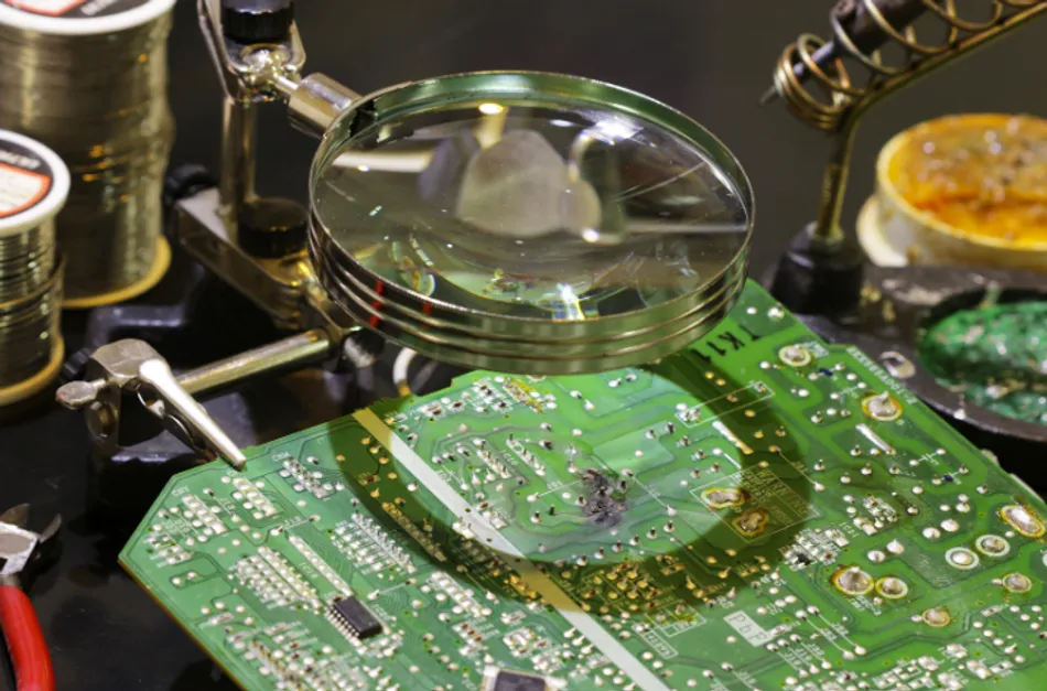
Inspection and Quality Control
Visual Inspection
Visual inspection stands as a pivotal stage in the quality assurance process for surface mount soldering, entailing a thorough examination of solder joints and components on circuit boards to spot defects or irregularities that might compromise the assembled electronic devices' performance and reliability. This inspection can be executed either manually or with the assistance of automated optical inspection (AOI) systems.
Manual Visual Inspection: Human operators meticulously scrutinize PCBs under magnification, relying on their expertise to discern potential defects. While allowing for human judgment, manual inspection is time-intensive and prone to errors, necessitating skilled operators to ensure consistent and accurate results.
Automated Optical Inspection (AOI): AOI systems leverage cameras, lighting, and image processing software to automatically scrutinize PCBs for defects. These systems compare captured images with predefined criteria to pinpoint anomalies swiftly and accurately. Offering enhanced speed, precision, and repeatability, AOI surpasses manual inspection in various aspects.
Defect Detection: Both manual and automated inspections aim to spot an array of soldering defects, including:
- Solder Bridges: Unintentional connections between solder joints that can lead to short circuits.
- Insufficient Solder: Inadequate solder volume on joints, resulting in weak mechanical and electrical connections.
- Excessive Solder: Excessive solder on joints, potentially causing short circuits or affecting neighboring components' performance.
- Component Misalignment: Misplaced components can cause poor electrical connections or strain on solder joints.
Post-Inspection Actions: Following visual inspection, any detected defects must be rectified through rework processes, such as desoldering and resoldering components or removing excess solder. Documenting inspection results and rework actions is crucial for traceability and process enhancement.
In essence, visual inspection plays a pivotal role in upholding the quality and reliability of surface mount soldering. Whether employing manual or automated methods, manufacturers can identify and rectify soldering defects, thereby enhancing their electronic products' performance and longevity.
Click to find out more
Comments