


In today’s rapidly advancing technological world, electronic devices have become indispensable in our daily lives. From smartphones and medical devices to industrial machinery and automobiles, every modern gadget relies on a critical component — the PCB circuit board assembly. This process forms the heart of electronic manufacturing, ensuring devices function efficiently, reliably, and safely.
What is PCB Circuit Board Assembly?
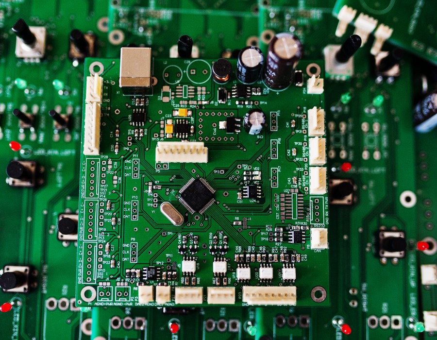
PCB stands for Printed Circuit Board, a platform that mechanically supports and electrically connects electronic components using conductive pathways, tracks, or signal traces etched from copper sheets. The PCB circuit board assembly process involves mounting electronic components such as resistors, capacitors, and integrated circuits onto the board to create a fully functional electronic device.
The assembly stage transforms a bare PCB into an operational system capable of performing specific tasks. This intricate process requires high precision, quality control, and modern manufacturing techniques to ensure the final product meets stringent performance standards.
Key Steps in PCB Circuit Board Assembly
The assembly process can vary depending on the design complexity and the intended application, but the main steps typically include:
1. Solder Paste Application
The process begins with applying a thin layer of solder paste onto the areas where components will be placed. A stencil printer is used to ensure accurate application on the copper pads.
2. Component Placement
Once the solder paste is applied, automated pick-and-place machines accurately position electronic components on the PCB. These machines use vision systems to ensure proper alignment, especially for surface-mount devices (SMDs).
3. Reflow Soldering
In surface-mount technology (SMT) assembly, the next step is reflow soldering. The PCB passes through a reflow oven where heat melts the solder paste, creating strong electrical and mechanical connections between components and the board.
4. Inspection and Quality Control
Automated Optical Inspection (AOI) systems are used to detect soldering defects, component misplacements, or bridging issues. This step ensures the assembled board meets high-quality standards before moving forward.
5. Through-Hole Component Insertion (if applicable)
For boards that require through-hole components (common in power electronics or connectors), components are inserted manually or by machine and soldered using wave soldering or selective soldering methods.
6. Functional Testing
Before packaging, assembled PCBs undergo functional testing to verify that all components operate correctly. Testing may include in-circuit testing (ICT), flying probe testing, or burn-in testing depending on the complexity of the design.
Types of PCB Assembly Technologies
There are primarily two types of PCB circuit board assembly technologies:
- Surface Mount Technology (SMT): Components are mounted directly onto the surface of the PCB. SMT allows for smaller, lighter, and more complex boards, making it ideal for modern compact electronics.
- Through-Hole Technology (THT): Components have leads that pass through drilled holes in the board and are soldered on the opposite side. THT provides robust connections, suitable for high-power or mechanically stressed applications.
In many cases, hybrid assembly combines both SMT and THT techniques to meet specific performance and design requirements.
Importance of PCB Circuit Board Assembly in Electronics
Without effective PCB assembly, even the most innovative circuit designs would remain theoretical. Proper assembly ensures:
- Reliability: Each component is securely attached and performs optimally under various conditions.
- Compact Design: Advanced assembly techniques enable miniaturization of electronics.
- Enhanced Performance: Accurate soldering and placement minimize electrical resistance and signal loss.
- Cost Efficiency: Automated assembly reduces human error and manufacturing costs while improving production speed.
Industries such as aerospace, healthcare, telecommunications, and automotive depend heavily on precise and reliable PCB assemblies for mission-critical systems.
Challenges in PCB Assembly
Despite technological advancements, the process still faces challenges like miniaturization, component shortages, and thermal management. As devices become smaller and more complex, manufacturers must adopt advanced inspection systems, robotics, and AI-driven quality control to maintain precision.
Additionally, environmental concerns are leading to the adoption of lead-free soldering and eco-friendly materials, aligning PCB manufacturing with global sustainability standards.
The Future of PCB Circuit Board Assembly
The future of PCB circuit board assembly lies in automation, artificial intelligence, and flexible electronics. Smart factories are increasingly utilizing machine learning algorithms to predict defects and optimize production. Meanwhile, innovations such as 3D-printed PCBs and flexible substrates are expanding the possibilities for wearable and IoT devices.
As technology evolves, PCB assembly will continue to play a pivotal role in driving innovation, efficiency, and connectivity across industries.
Conclusion
The PCB circuit board assembly process is the cornerstone of the electronics industry, turning conceptual designs into tangible, high-performing devices. Through precision engineering, advanced technology, and rigorous quality control, PCB assembly ensures that modern electronics continue to shape the world we live in — from communication and healthcare to transportation and beyond.
Comments